SemiconductorHard
Question
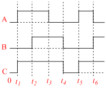
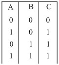
The figure shows a logic circuit with two inputs A and B and the output C. The voltage wave formsacross A, B and C are as given. The logic circuit gate is
Options
A.NAND gate
B.OR gate
C.NOR gate
D.AND gate
More Semiconductor Questions
In a full wave rectifier circuit operating from 50 Hz mains frequency , what is thefundamental frequency in the ripple ?...The logic symbols shown here are logically equivalent to : -(a) (b)...If the highest modulating frequency of the wave is 5kHz, the number of stations that can be accomdated in a 150 kHz band...What will be the input of A and B for the boolean expression = 1 : -...A two Volts battery forward biases a diode however there is a drop of 0.5 V across the diode which is independent of cur...