SemiconductorHard
Question
The logic symbols shown here are logically equivalent to : -
(a) (b)
(b) 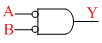
(a)
(b) Options
A.′a′ AND and ′b′ OR gate
B.′a′ NOR and ′b′ NAND gate
C.′a′ OR and ′b′ AND gate
D.′a′ NAND and ′b′ NOR gate
More Semiconductor Questions
Which element is to be mixed in germanium to make acceptor type semiconductor : -...In a p-n junction the reverse saturated current is 10−5 ampere at 27o C. The value of forward current for it at 0....When two semiconductor of p and n type are brought in to contact, they form a p-n junction which acts like a : -...If the lattice constant of this semiconductor is decreased, then which of the following is correct?...The circuit shown in contains two diodes, each with a forward resistance of $50\ \Omega$ and infinite backward resistanc...