SemiconductorHard
Question
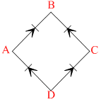
In the figure, input is applied across A and C and output is taken across B and D, then the output is :
Options
A.zero
B.same as input
C.full wave rectified
D.half wave rectified
More Semiconductor Questions
Which value of potential barrier is in the range, for given PN junction :-...A NAND gate followed by a NOT gate is :-...The depletion region of a p-n junction contains : -...The following figure shows a logic gate circuit with inputs A and B and the output Y. The voltage waveform of A, B and Y...Mobility of electrons in N-type Ge is 5000 cm2/volt sec and conductivity 5 mho/cm. If effect of holes is negligible then...