SemiconductorHard
Question
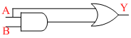
The truth table for the following combination of gates is
(a) (b)
(b)  (c)
(c)  (d)
(d) 
(a)
(b) (c) (d) Options
A.a
B.b
C.c
D.d
More Semiconductor Questions
Pure Si at 500 K has equal number of electron (ne)and hole (nh) concentration of 1.5 × 10¹⁶ m-3. Doping by indium increa...A transistor is used as an amplifier in CB mode with a load resistance of 5 kΩ the current gain of amplifier is 0.9...An amplifier has a voltage gain Av = 1000. The voltage gain in dB is :...Which of the following relations is valid for Boolean algebra : -...In communication with help of antenna if height is double then the range covered which was initially r would become...