SemiconductorHard
Question
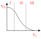
Transfer characteristics [output voltage(V0) vs input voltage (Vi)]for a base biased transistor in CE configuration is as shown in thefigure. For using transistor as a switch, it is used
Options
A.in region I
B.in region III
C.both in region (I) and (III)
D.in region II
More Semiconductor Questions
The voltage gain of the following amplifier is...What will be the input of A and B for the boolean expression = 1 : -...When all the inputs of a NAND gate are connected together, the resulting circuit is : -...The majority current in a p-n junction is :-...Electric conduction in a semiconductor takes place due to : -...