SemiconductorEasy
Question
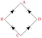
For the given circuit shown in fig, to act as full wave rectifier :- a.c. input should be connected across ................. and ..................... the d.c. output would appear across ................ and .....................
Options
A.A, C, B, D
B.B, D, A, C
C.A, B, C, D
D.C, A, D, B
More Semiconductor Questions
on increasing the temperature of semiconductor, its resistance :-...Assuming in forward bias condition there is a voltage drop of 0.7 V across a silicon diode, the current through diode $D...The region of trasistor in which extra impurity is doped to obtain a large number of majority carrier is called as: -...The input resistance of a silicon transistor is 100 Ω. Base current is changed by 40 mA, which resultsin a change i...Mobility of electrons in N-type Ge is 5000 cm2/volt sec and conductivity 5 mho/cm. If effect of holes is negligible then...